With the by now extensive knowledge about materials and how to manipulate their superconducting properties, it was also clear how. While the high sensitivity of an aluminium KID is ideal for detecting extremely weak signals in “difficult” radiation wavelengths, such as those below one millimetre, an antenna made of niobium titanium nitride (NbTiN) is excellent as a stable energy conductor to the detector without loss. It keeps out all kinds of noise that aluminium is less able to cope with.
“NbTiN is the ideal material for making the filters that Akira needed. Teun Klapwijk developed it in the 1990s for the ALMA and Herschel detectors, and with the KIDs it is once again playing a major role in astronomy,” says Baselmans.
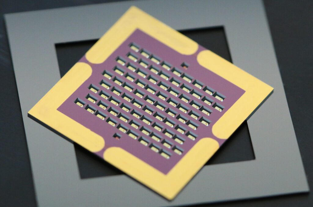
Productive pioneering: manufacturing on ever higher levels
But now it was time to get building. That came with its own set of challenges. David Thoen: ‘We were venturing into unknown territory; this had never been done before. Teun Klapwijk always said: “Make as many mistakes as possible in as little time as possible”, and that’s what we did,’ he says.
“An aluminium detector or a 200-nanometre NbTiN antenna wire (roughly one-fourth the thickness of a human hair) cannot hang in the air. But where to put it on, keeping signals in the circuit unaffected by the substrate underneath?” One path we tried but then abandoned, for example, was micrometre crystalline silicon membrane. ‘Extremely thin, but also extremely fragile. Thinking back to the breaking crystalline silicon and the film on top of it can still get me nervous again,’ says Thoen. A more robust solution was found in membranes made of ‘amorphous’ material, i.e. without the fragile ordered crystal structure.
‘That was a journey that took years. We had to fine-tune the machines and test how those layers functioned at all colours and frequencies. But there were no test setups for far infrared to check the quality, so Akira Kenichi and I installed all equipment to an empty lab in TU Delft and established a way to efficiently test fabricated chips.’
Another important aspect of the manufacturing process that took years to develop is the uniformity of the layers on the chip, says Thoen. ‘You want the layers to have the thickness you intended in the design at every point on the chip, rather than them being thicker in the middle and thinner towards the edges of the chip, where they would have a different resistance. This is particularly important for larger arrays with thousands of KIDs on them.’ A new Evatec machine was used to achieve uniform resistivity across the entire wafer.
In addition to uniformity, the control of line thicknesses and detailing of patterns in the chips also ramped up. ‘We now make line widths of 250 nanometres and can, for example, create almost perfectly right-angled structures, while the results are increasingly predictable. The quality and reproducibility of what we make is enormous. We are in complete control of what we are doing.’